An AI accelerator is more than its processor die. It must move data from memory into compute units, move results between dies, and deliver power while removing heat. A faster transistor helps, but a slow or power-hungry connection can leave that transistor waiting. That is why advanced packaging AI chips has become a useful search question: the package increasingly determines how much of a chip’s theoretical performance a complete system can use.
Packaging once sounded like the final protective step after fabrication. Today it can be a design choice made alongside the processor itself. Multiple dies may sit beside one another on an interposer, memory may be placed close to logic, and some dies may be stacked vertically. Each arrangement changes the distance, density, and energy cost of moving information. This guide explains the engineering trade-offs and how to assess announcements without confusing a prototype with reliable production.
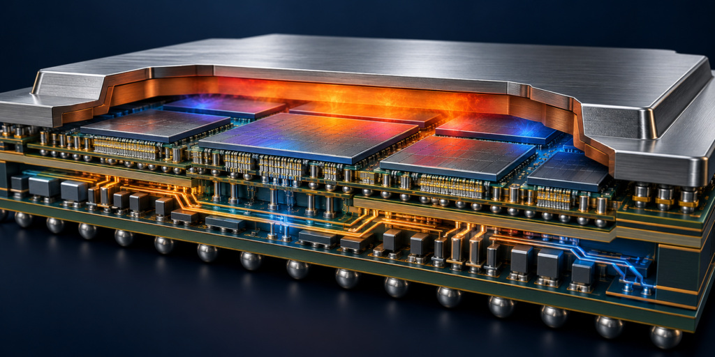
What advanced packaging actually connects
The word die refers to an individual piece cut from a processed wafer. A conventional package gives that die electrical connections and physical protection. Advanced packaging connects several functional components inside one package, often through finer interconnects than a circuit board can provide. Those components may use different manufacturing processes: leading-edge logic, mature-node input/output circuits, and stacked memory do not all benefit equally from the same process node.
TSMC describes its 3DFabric portfolio as including SoIC, CoWoS, and InFO, spanning stacking and backend packaging services. These are company-specific technologies, not interchangeable names for every package. Likewise, Intel Foundry’s packaging overview distinguishes its EMIB bridges and Foveros stacking approaches. A reader comparing advanced packaging AI chips should ask which components are connected, how they are connected, and whether the example is in volume production.
Chiplets and the role of an interposer
A chiplet is a die intended to operate with other dies as part of a larger system. Splitting functions can let designers select appropriate processes for each component and reuse proven blocks. The benefit depends on the connections: dividing a design creates communication between pieces that previously might have communicated within one die. An interposer or embedded bridge supplies dense pathways for some of those signals; it does not make distance or energy costs disappear.
TSMC’s CoWoS description identifies versions using a silicon interposer, redistribution-layer interposer, or local silicon interconnects. Its examples connect logic and high-bandwidth memory within a package. Intel explains that EMIB links dies placed side by side, while Foveros supports vertical stacking. These architectures solve related integration problems through different physical designs; a product comparison needs actual bandwidth, power, cost, and manufacturing evidence.
Why high-bandwidth memory is nearby
AI workloads repeatedly exchange model data and intermediate results with memory. High-bandwidth memory, or HBM, uses stacked memory dies and wide connections near the processor. Its value is the ability to move large amounts of data efficiently across short package-level paths. That does not mean every workload is memory-bound, or that adding memory automatically doubles useful throughput. The compute architecture, software, capacity, and movement between accelerators still matter.
TSMC says its CoWoS-S implementation accommodates logic chiplets and HBM stacks on a silicon interposer. Its 2025 annual-report technology discussion also describes CoWoS as integrating system-on-chip components and HBM to improve computing and memory bandwidth. These are evidence for what the technology integrates, not an independent benchmark proving that every accelerator using it performs better.
Why scaling has become a system problem
Smaller transistors can increase density and improve some performance or power characteristics. Yet an AI system also depends on memory supply, inter-die signaling, power delivery, cooling, and software. If a processor can perform calculations faster than data can arrive, more compute units may sit idle. If a connection consumes too much energy, the power budget can limit operating speed. Advanced packaging AI chips addresses those constraints by bringing components closer and increasing connection density, while adding its own design and manufacturing challenges.
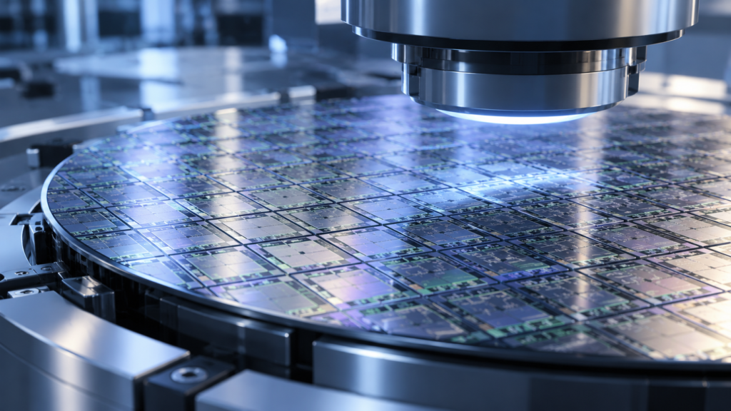
High-NA EUV belongs to a different part of this story. ASML’s EUV systems page describes lithography equipment used to print fine features during wafer fabrication. Packaging later assembles and connects completed dies. Both may advance AI hardware, but calling High-NA a packaging method would mix two stages of production. A new lithography capability also does not remove the need to design memory links, power paths, and thermal management for the finished system.
Bandwidth, latency, and power are separate questions
Bandwidth measures how much data a connection can transfer over time; latency describes how long a particular transfer takes. A design can improve one without proportionally improving the other. Engineers also consider energy per transferred bit and the heat produced by densely assembled components. Consequently, an announcement about peak bandwidth is only part of the evidence needed to predict workload performance.
For advanced packaging AI chips, ask which path the claim describes. Is it logic-to-HBM bandwidth inside a package, die-to-die communication, or networking between servers? Those paths have different physical limits and different effects on an application. A vendor’s laboratory result for one path should not be described as the speed of an entire data center. Useful comparisons specify the tested product, workload, measurement conditions, and power consumption.
More connections also mean more failure points
Combining dies creates alignment, bonding, testing, and thermal-management work. Each component needs to function, and the assembled system must survive the manufacturing process and operate reliably. A larger package or more elaborate stack is therefore not automatically an economical choice. Testing components before assembly can reduce the risk of combining a defective die with good ones, but final-package testing remains necessary.
TSMC’s SoIC account discusses integrating known-good dies of different sizes, functions, and process technologies. Its description supports the design concept; it does not disclose a universal yield for all customer products. Advanced packaging AI chips should be evaluated on usable output and cost per working system as well as on physical interconnect density. Those figures often depend on a design and may not be publicly disclosed.
Where packaging fits in the manufacturing chain
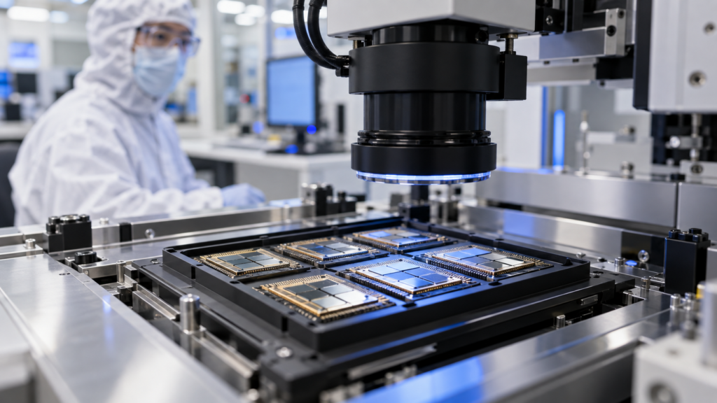
Chip design defines functions and connections. Wafer fabrication builds the dies. Assembly places or stacks them and forms the package connections. Testing occurs at multiple points, including checks of the finished device. A company may participate in one stage or coordinate several suppliers. This division matters when people speak loosely of a “chip shortage”: additional wafer output alone may not create finished accelerators if memory, packaging, or final testing capacity is constrained.
The Semiconductors pillar introduces design, fabrication, and industry challenges. The TSMC company profile gives foundry context, while the Applied Materials and Lam Research profiles cover equipment suppliers. These company pages answer who participates in the industry; the question here is how component integration changes an AI processor’s possible performance and production economics.
Capacity is more specific than a factory announcement
When a supplier announces a facility or technology for advanced packaging AI chips, separate planned investment from installed tools, qualified processes, production starts, and delivered working packages. A statement about potential capacity may refer to a future line, a particular package type, or output before testing losses. It need not translate directly into finished accelerators available to buyers. Memory supply and a customer’s completed chip design can affect that translation too.
The 2025 TSMC annual report reports that its 3nm SoIC stacking technology entered volume production in 2025. That is a dated statement about a specified technology. It should not be generalized into a claim that every announced 3D package is already shipping at scale. For advanced packaging AI chips, the distinction between an available manufacturing service and a particular customer product is essential.
A practical way to assess a packaging claim
Start by identifying the physical arrangement. Are logic dies side by side, stacked, or connected through an interposer? Where is HBM located, and which link is supposed to improve? Next identify the stated advantage: capacity, bandwidth, lower connection energy, more design flexibility, or a smaller footprint. Treat each as a separate proposition requiring its own measurement.
Then check the status of the evidence. A company technology page can explain the design, but it is written by the seller. A technical paper may describe a working demonstration. A dated annual report or filing can establish what a company says entered production during a specified period. None alone proves a buyer’s realized workload performance, price, or delivery date. If a claim is a forecast, label it as one and return to it when production data becomes available.
Finally, examine trade-offs in advanced packaging AI chips. Stacking may shorten some links but intensify thermal questions. Breaking one large die into chiplets may improve design flexibility while making die-to-die communication and package assembly more important. Dense connections may improve bandwidth but require specialized manufacturing and testing. Advanced packaging AI chips is therefore a set of engineering choices, not a guarantee of cheaper or faster compute in every configuration.
What the next reader should watch
The most informative developments are measurable: a named product entering volume production, a specified memory configuration, benchmark results under disclosed conditions, and evidence that suppliers can repeatedly deliver working packages. Compare claims over time using the same units and the same stage of production. A larger package footprint or an impressive transistor count does not by itself establish usable system performance.
Advanced packaging AI chips matters because AI computing depends on how logic, memory, and power function together. Transistor advances remain valuable; package architecture determines whether several advanced components can operate as a coherent, manufacturable system. The sound question is not which technology replaces the other. It is which constraint a particular design removes, what new constraint it introduces, and whether its demonstrated output justifies the added complexity.